| Laser and Photonics |
 Laser Diode and DPSS Laser system Laser Diode and DPSS Laser system |
| High Power Tunable External Cavity Diode Lasers |
| Nd:YAG Laser Systems |
| Spectral Products & CVI Laser |
| Excimer Lasers |
| Synrad Lasers |
| Calibration and Measuring Instruments |
| Gauge Calibration Instruments |
| Flatness and Roughness Interferometer |
| Corning Tropel Interferometer system |
| Mask Aligner & Spin Coater equipment |
| Imaging and Spectroscopy system |
| PCO Imaging High Performance Camera system |
| Customer Laser Spectroscopy and High Resolution Imaging System |
| Cryogenic |
| Industrial and Manufacturing |
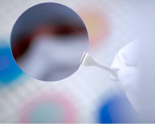
| Epitaxy
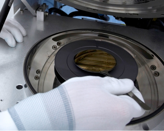
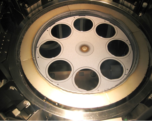
Epitaxy is a field of professional competence offered by Jenoptik. Devices based on Jenoptik epitaxial wafers in the Al-Ga-In-As-P material system have proven their quality in numerous products. Additional to our laser products, we provide customized epitaxy services in the production of thin semiconductor layer structures, i.e. epitaxy of layer structures on GaAs wafers. In accordance to your specifications, we are able to deliver epitaxial wafers with guaranteed high-quality epitaxial growth of layer structures on 2”, 3”, and 4” wafers. Production of epitaxial wafers
Our monitored MOCVD / MOVPE production process with tight quality control ensures consistently high quality from start to finish. PDF Epitaxial wafer services (168 KB)
For any questions regarding our epitaxial services or for comprehensive consulting, please contact us. We are happy to assist you. |
.jpg)